Eliminating Surface Roughness in Electronic Substrates
Surface roughness is a property that defines the three-dimensional (3D) structure of a substrate’s uppermost surface layers. It is a complex characteristic that is typically characterized by material-specific features or process marks – or a combination of the two. In the context of electronic substrates, surface roughness is an intermediary property that must be eliminated through a careful and highly technical, chemically-assisted polishing processes.
In this blog post, we will explore the elimination of surface roughness from electronic substrates in more detail.
The Problem with Surface Roughness
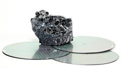
The problem with surface roughness in electronic substrates is the perpetual industry trend towards device miniaturization and increased electronic density. This demands circuitry with high-performance integrated electronic features (transistors, resistors, conductors, etc.) that have mere micro- (μm) and nanoscale (nm) geometries. Tandem innovations in substrate growth and wafer extraction, and high-precision vacuum processes – such as chemical vapor deposition (CVD) and photolithography – have enabled manufacturers to successfully print extraordinary electronic subsystems in smaller formats than ever before.
Importance of Polishing Processes in Microelectronics
Achieving Planarization of Electronic Substrates
This precision mandates absolute planarity, as even sub-microscale material features can influence key desirable properties of electronic substrates. Tests have found links between surface roughness and poor adhesion, electrical properties, wettability, and more. Contributing features may include process scratches propagated from slicing, sawing, and preceding polishing steps, or simply natural roughness from the substrate’s microstructure.
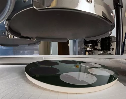
Chemical mechanical planarization (CMP) is a critical enabling technology in the field of semiconductors and printed electronics. It provides the means for chemically-assisted polishing that eliminates the risk of creating new surface defects due to abrasion by polishing pads or abrasive particles. This comes down to the use of compound slurries that suspend hard-wearing particles in an appropriate solution, facilitating desirable chemical reactions at the substrate interface which create structurally weaker compounds that can then be removed via abrasion.
Slicing Grinding & Finishing: Outlining Surface Preparation of Electronic Substrates
Saint-Gobain Surface Conditioning offers a range of slurries suitable for multiple steps in the CMP process, from the pre-polish stage onwards. The format of these is dependent on the substrate material in question, but we can reliably provide a suite of polishing slurry solutions for a comprehensive range of materials.
Eliminating surface roughness in your electronic substrate must be handled holistically. At Saint-Gobain, we operate on a customer-first basis to carefully match the right product to the right process. If you would like more information about how to eliminate surface roughness in your proprietary substrates, simply contact a member of the Saint-Gobain team today.