
Slicing, Grinding & Finishing: Outlining Surface Preparation of Electronic Substrates
Surface preparation is an essential process for achieving the high-precision end-use qualities of electronic substrates. This extends beyond simply polishing substrates with an abrasive slurry and impacts every step of the manufacturing process from crystal growth onwards. Slicing, grinding, lapping, and polishing must all be individually optimized as part of a broad review of your surface preparation methodology.
In this blog post, Saint-Gobain Surface Conditioning outlines the general process of electronic substrate surface preparation.
Introduction to Substrate Growth
At Saint-Gobain, we do not grow crystals. We cultivate a close network of partners and customers that are the experts in crystal growth for the electronics market. Working with market leaders helps us provide tailored surface preparation services for advanced substrate materials
Slicing Single-Crystal Ingots
Once a crystal is grown, finishing steps can begin. The first process in electronic substrate surface preparation is slicing, where thin wafers are extracted from the cylindrical ingot using a diamond or alternative abrasive wire saw. This uses a continuous length of thin wire in tandem with loose or fixed diamond particles, providing high cutting rates with exceptional surface uniformity due to the inherent hardness of the diamond abrasive and the chemical properties of the coolant. Engineered slurries or fixed diamond wire cutting can both provide appreciable cost savings for sawing extremely hard crystal ingots like silicon carbide. However, we can offer solutions regardless of whether or not our customer is using fixed diamond wire or a loose abrasive.
Grinding & Lapping Electronic Wafers
Substrate lapping is effective for achieving a high quality, defect-free surface finish of electronic substrates. This precedes polishing, utilizing a fine-particle abrasive slurry and low-speed rotational force to remove minute amounts of surface material from the electronic wafer. Subsurface damage can be eliminated without imparting new mechanical flaws, reducing the risk of defects propagating to the finished product. In the case of silicon carbide, we can provide both lapping and a pre-polish stage to guarantee a defect-free surface for the final stage of surface preparation.
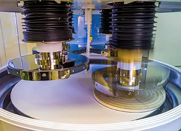
Polishing and CMP
Chemical mechanical planarization (CMP) is one of our core competencies at Saint-Gobain Surface Conditioning. This is the process of leveling the surface topology of electronic substrates using a combination of mechanical force and chemical reactions. We offer polishing and CMP slurries with finely-developed nanoparticles, providing tailored chemistries and particle morphologies to the substrate material of interest.
Staying with the example of silicon carbide (SiC), we offer the ClasSiCTM CMP and polishing slurries for silicon carbide surface preparation and finishing. This facilitates exceptional material removal from the surface with excellent planarization performance.
Surface Preparation with Saint-Gobain Surface Conditioning
Saint-Gobain Surface Conditioning is one of the world’s leading authorities in high-technology surface preparation. We understand the distinct chemical and mechanical requirements of preparing electronic wafers from challenging crystallite materials as varied as sapphire (Al2O3), aluminium nitride (AlN), gallium nitride (GaN), and much more.
If you would like any more information about Saint-Gobain Surface Conditioning’s electronic substrate services and products, simply contact us directly.