Importance of Polishing Processes in Microelectronics
Microelectronics are embedded into practically every aspect of modern life, from personal devices to large-scale infrastructural controllers. The term is often used to describe electronic components with extremely small dimensions; specifically, components with microscopic elements (capacitors, conductors, diodes, inductors, resistors, transistors, etc.). Because of their tiny geometries, the margins of success in microelectronics are incredibly tight. Device preparation and process control are paramount for meeting the growing demands of an increasingly discerning consumer base.
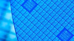
Polishing processes are a key preliminary step in fabricating integrated electronics, enabling the absolute planarization of electronic substrates prior to etching/deposition. In this post, Saint-Gobain will explore why the polishing process is so critical to success in modern microelectronics.
A Brief History of Microelectronics
Although ubiquitous today, the history of microelectronics can only be traced back as far as 1947 and the invention of the germanium point-contact transistor. This device comprised a germanium slab and a point contact shielded with two distinct leaves of gold foil. The experiment established semiconductor materials as a crucial component for microelectronics going forward, but it took decades for mainstream markets and even scientific sectors to appreciate the potential of the transistor.
The device went through several iterations until planar technologies were conceived in the late ‘50s, building to early successes into the fabrication of integrated circuits (ICs) and ultimately the invention of planar electronics. This is where polishing processes became fundamental to success. Most manufacturers of integrated and monolithic integrated circuits made use of MOS (metal oxide semiconductors) technology as the basis of logic, memory, and processing boards – to name a few applications. However, these devices were still comparatively large scale compared to today’s standards, and there was no single polishing process diagnosed for best substrate planarization.
The drive towards device miniaturization and higher density electronics is hardwired into the history of circuitry. As devices decreased in both size and increased density, the need to remove even the tiniest topographical variations became much more prevalent. This coincided with new fabrication techniques (additive patterning, photolithography, etc.) and vacuum processing that could guarantee nanoscale levels of precision with reasonable certainty. Before these methods were established, polishing processes like chemical mechanical planarization (CMP) were considered unsuitable for microfabrication.
Nowadays, CMP polishing processes are ideal for substrate planarization due to technology’s ability to generate uniform surfaces with outstanding discrimination between interfacial layers (i.e. underlying semiconductor and surface oxides). It has risen from an outlying technology in high precision fabrication to a fundamental process in electronic substrate surface preparation. If you would like to learn more about how CMP polishing processes have become increasingly instrumental in a changing world of electronics, read our previous blog post Chemical Mechanical Planarization: Enabling New Electronics.
Electronics Polishing Processes from Saint-Gobain
Saint-Gobain Surface Conditioning is a world leader in advanced CMP polishing processes for electronic substrates. We offer vertically integrated solutions to guarantee ultra-precise topographical planarity for semiconductor wafers of even the hardest wearing substrate materials.
If you would like more information about the polishing processes that we can assist with, simply contact a member of the Saint-Gobain team today.