CMP and Integrated Circuits
Chemical mechanical planarization, usually abbreviated to CMP, has proven an enabling technology for the increasingly diverse field of semiconductor devices. It was initially discounted for precision polishing applications but has become a mainstay in the development of complementary metal-oxide-semiconductors (CMOS) and planar substrates for integrated circuits (ICs).
CMP: A Versatile Polishing Solution
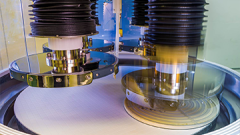
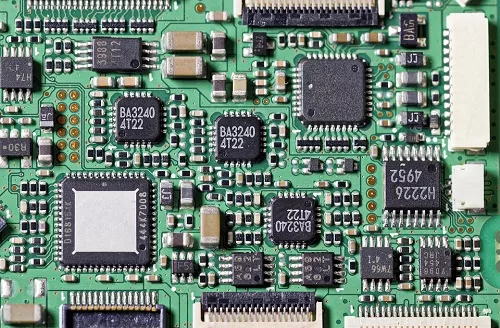
Integrated circuits are often called ‘chips’, a term that refers to substrate materials that have been extracted from semiconductor ingots. These wafers are acquired through extremely high-precision techniques (i.e. diamond wiresaw cutting), yet, even nanoscale topographical variations in electronic substrates can cause yield-limiting problems in subsequent process steps (i.e. additive manufacturing). The purpose of CMP is to planarize substrates after extraction for ultra-flatness, improving workflows to satisfy the demands of an enormous global market.
This outstanding level of performance extends from conventional semiconductor materials to new, emerging, and proprietary substrates. At Saint-Gobain, we are well-equipped to perform CMP polishing of wafers as varied as:
• Aluminum nitride (AlN)
• Gallium compounds, including gallium arsenide (GaAs), gallium nitride (GaN), and gallium oxide (Ga2O3)
• Indium phosphide (InP)
• Lithium niobite (LN) and lithium tantalite (LT)
• Sapphire (Al2O3)
• Silicon
• Silicon carbide (SiC)
• Silicon nitride (SiNx)
• Quartz (SiO2)
The reason why CMP processes have demonstrated such longevity in the field of semiconductor manufacturing is the chemical specificity of each individual substrate material. CMP relies on a combination of chemical reactions and sustained mechanical agitation to remove surface reactants from wafers and provide a planar surface for subsequent manufacturing steps. These reactions are facilitated by substrate-specific slurries and process-optimized pads to exploit the unique chemistry of each individual wafer and guarantee planarization for optimal processing conditions.
As a result, CMP has become embedded in the foundations of IC technology, facilitating a new generation of microelectronics. If you would like to learn more about this, read our previous blog post on the Importance of Polishing Processes in Microelectronics.
CMP Polishing with Saint-Gobain Surface Conditioning
The unique capabilities of CMP processes continue to provide high-performance substrates for increasingly demanding market segments. Saint-Gobain Surface Conditioning specializes in the polishing processes that ultimately make modern electronics function, helping you improve your workflows by maximizing throughput with diminished defectivity for appreciable returns on investment in your production line.
Are you looking to improve your IC development workflow in a cost-effective manner? Contact a member of the Saint-Gobain team today. With decades of experience in CMP polishing, we are confident that we can handle your substrate and reduce overall device costs.