Downstream Applications of CMP Polishing
Chemical mechanical planarization (CMP) is a high-precision manufacturing technique used to remove minute volumes of surface material from substrates via chemically-assisted abrasion. It is primarily an intermediary manufacturing process that produces topographically-uniform semiconductor wafers for electrical and electronic equipment (EEE).
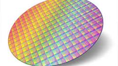
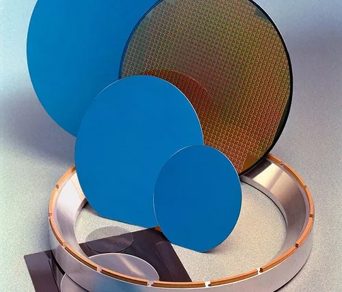
In the context of electrical and electronic equipment, a wafer is a thin slice extracted from a semiconductor ingot like silicon (Si) – the eponymous electronic material of the modern age. Once planarized via CMP, these wafers go on to serve numerous advanced roles in consumer goods and energy generation. In this blog post, Saint-Gobain Surface Conditioning will introduce some of the downstream applications of CMP polishing in more detail.
What is CMP Polishing and Why is it Used?
As mentioned, CMP is an intermediary manufacturing step in the semiconductor production chain, following on from crystal growth and wafer extraction. The polishing process overarches two primary inter-connecting purposes: Material removal and planarization.
Learn more about the semiconductor wafer production chain: Wire Sawing for Electronic Substrate Slicing
Material removal, the first purpose of CMP polishing, is primarily concerned with key parameters such as slurry particle composition and geometry, pad asperity, and – consequently – the unique physicochemical interactions between the substrate and other elements of the process. Finely tailoring these parameters enables the accurate removal of topographical surface variations from a substrate to achieve planarization – the second purpose of CMP polishing. Achieving high levels of planarization requires a thorough understanding of surface feature evolution under given process conditions.
Highly-skilled CMP professionals with the right equipment can achieve absolute planarity with nanometer (nm) levels of accuracy to satisfy the precise demands of various downstream applications. To read more about the importance of this process, read our previous blog post Slicing, Grinding & Finishing: Outlining Surface Preparation of Electronic Substrates.
Processes Downstream of CMP Polishing
The chief application of CMP polishing is the electronics industry, which has grown increasingly diverse since the widespread genesis of semiconductors and vacuum processing technologies. It is now possible to generate nanoscale structures on uniform substrates using a plethora of high-precision techniques, typically based on either deposition or photolithography.
Photolithography refers to the use of a light-sensitive polymer overlaid on a substrate, known as a photoresist, which is selectively exposed to light to generate a pattern. This is commonly used to produce complex integrated circuits (ICs).
Thin-film deposition is broken down into two sub-families (physical and chemical) that further break down into distinct processes.
A selection of physical deposition techniques includes:
• Molecular beam epitaxy
• Radiofrequency (RF) sputtering
• Vacuum thermal evaporation.
Chemical deposition methods, meanwhile, include:
• Atomic Layer Deposition (ALD)
• Chemical vapor deposition (CVD)
• Spray pyrolysis
Each of these techniques requires a practically flawless substrate to generate electrical devices as varied as consumer displays, photovoltaic panels, wearable technologies, and more.
CMP with Saint-Gobain
Saint-Gobain Surface Conditioning is one of the world leaders in substrate surface preparation for various subsequent manufacturing stages. If you have any questions about the materials we can work with, or about the CMP process in general, please contact a member of the team today.